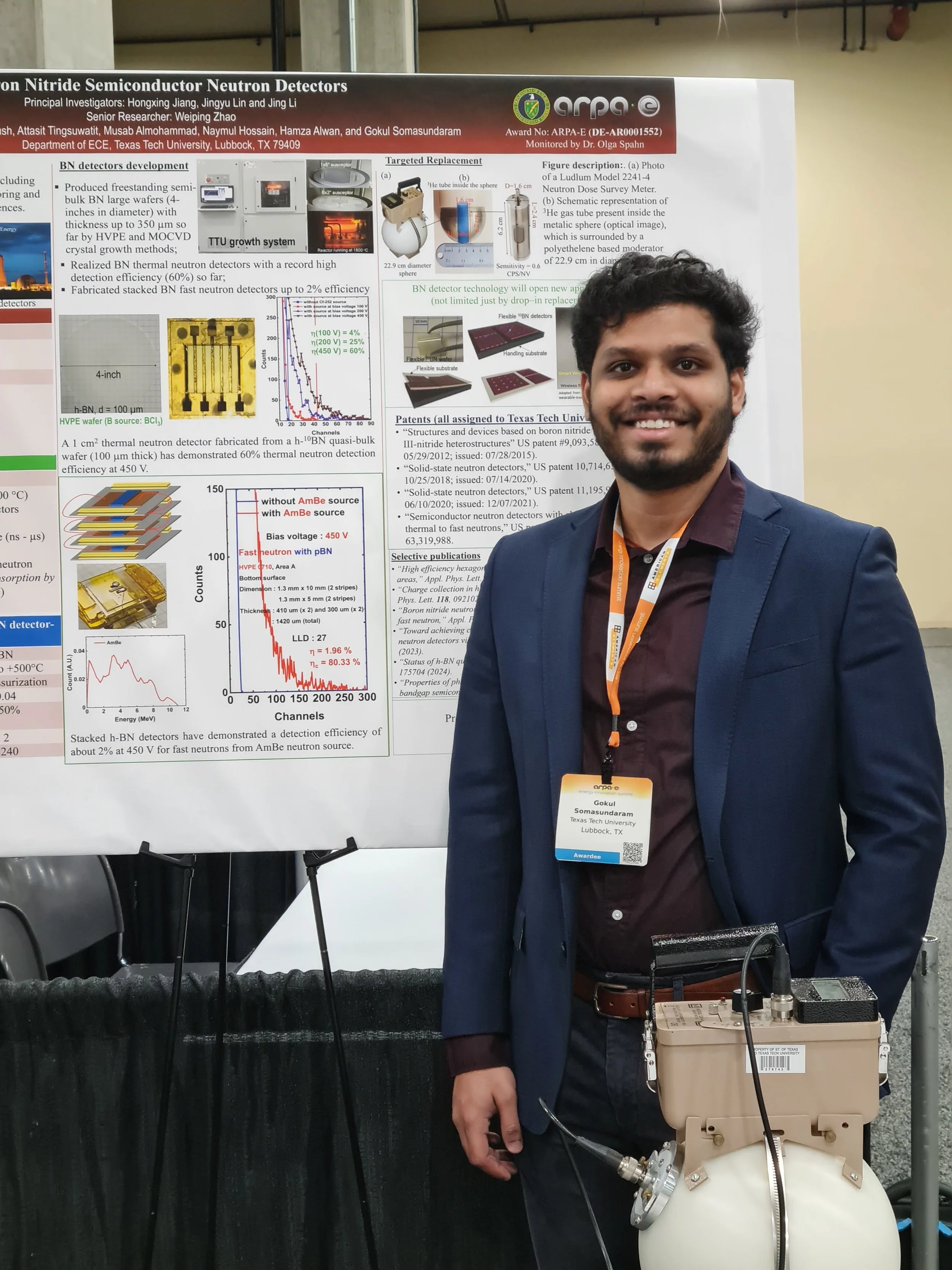
Micro/Nanofabrication | Semiconductor Devices & Materials Characterization
Process Development Engineer | RF Testing
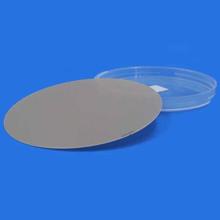
10+ Publications | 35+ Citations | h-BN | AlN | 14.1 MeV Neutron Detection
Electrical Engineering Ph.D. candidate with hands-on experience in semiconductor wafer processing, device fabrication, photolithography, dry etching, metallization, and electrical/optical characterization. Skilled in process development, optimization, troubleshooting, and data analysis for h-BN and AlN:Zr devices, with prior RF power-amplifier characterization experience at Skyworks Solutions
What I work on
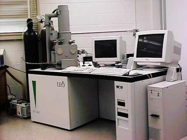
Semiconductor Process and Fabrication
Photolithography, ICP etching, metallization, annealing, wafer processing, packaging, and semiconductor process development
RF & Microwave Engineering
RF semiconductor technologies, device characterization, RF measurement and testing, circuit/device performance analysis, and experience within the RF semiconductor industry
Semiconductor Device Engineering
Electrical characterization, I–V measurements, breakdown analysis, photocurrent measurements, transport properties, high-voltage testing, and device optimization.
Ultrawide-Bandgap Semiconductor Research
Development of h-BN and AlN devices for radiation detection, high-field electronics, photoconductive switching, and emerging semiconductor applications.

Experiences
Publications

Awards
My Journey
〰️
My Journey 〰️
Anna University in Chennai, India, where I earned my Bachelor of Engineering in Electronics and Communication Engineering in 2020.
This foundation introduced me to electronics, communication systems, semiconductor devices, and RF engineering, and motivated me to pursue graduate studies in electrical engineering.
Texas Tech University, earning my Master of Science in Electrical Engineering in August 2023 with a GPA of 3.7.
My master's research focused on RF and microwave systems, specifically the linearization of millimeter-wave power amplifiers using Digital Predistortion (DPD).
This work strengthened my experience in RF power-amplifier characterization, measurement, data analysis, and device-performance optimization
Ph.D. in Electrical Engineering at Texas Tech University, where I currently maintain a 3.8 GPA and expect to graduate in May 2027.
During my doctoral studies, my research evolved toward semiconductor materials, device fabrication, charge transport, and radiation detection.
My Dissertation
〰️
My Dissertation 〰️
“Charge Carrier Transport and Fast Neutron Detection by Quasi-Bulk Hexagonal Boron Nitride,” focuses on understanding electrical transport in thick h-BN semiconductor devices and developing them for fast-neutron detection. Through this research, I have gained hands-on experience in semiconductor wafer processing, photolithography, dry etching, metallization, device fabrication, electrical and optical characterization, process optimization, and high-voltage testing.
My progression from RF and millimeter-wave electronics to semiconductor device processing and ultrawide-bandgap materials has given me a multidisciplinary perspective spanning RF characterization, semiconductor fabrication, device physics, experimental research, and advanced electronic materials. My goal is to apply this combination of skills to the development and manufacturing of next-generation semiconductor devices and technologies.